Advanced Quantum Devices Laboratory – AQDL is a new nanofabrication, test, and measurement facility dedicated to serving a wide community of academia and industry. The facility includes an anaerobic environment for nanolithography and device fabrication, exfoliated monolayer crystal positioning, patterning and transport measurements over a large range of temperatures, and up to 2.6 T magnetic field. Its operation is integrated with access to state of the art European nanofabrication facilities.
The laboratory is being managed jointly by the Department of Complex Matter at IJS together with CENN Nanocenter.
Contact person:
Damjan Svetin
tel: +386 1 477 3553
email: damjan.svetin@ijs.si
Location: Room B 106
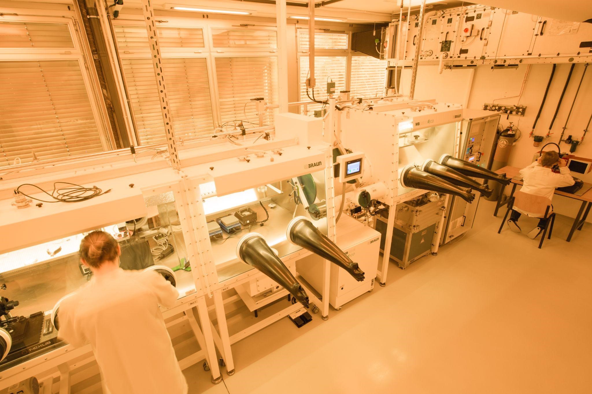
Glovebox with integrated equipment
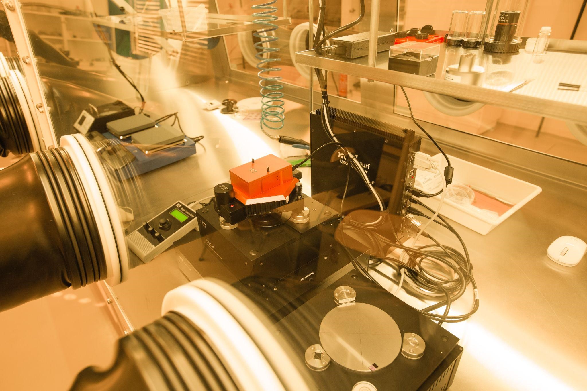
Glovebox with nitrogen atmosphere allows sample manipulation, preparation and characterisation, as well as device fabrication in an inert environment without the presence of oxygen and water (<0.1 ppm O2, <0.1 ppm H2O). It includes optical microscopes with precise translator stages for sample deposition and stacking of 2D materials, atomic force microscope (AFM) for sample characterisation, spin coater and hot plates for lithography procedures, and electron beam evaporator for evaporation of thin films of metals. It also allows for controlled transfer of samples in an inert atmosphere between different systems (STM, MBE) via a vacuum suitcase.
Details:
- Manufacturer: MBraun
- Components: 3x MB200MOD glovebox, MB-20-G-W-V2A gas purifier, MB-LMF-2/40 solvent contamination remover, HEPA 13 particle filters, yellow box light, BNC feedthrough connectors, optical microscopes, AFM, spin coater, hot plate, integrated evaporator
Electron beam evaporator
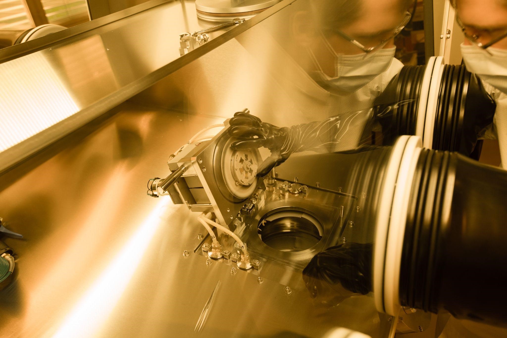
The system is designed for the evaporation of thin films of materials with assistance of electron beam (e-beam evaporation). 6kW e-beam source allows evaporation of the metals as Au, Pd, Al, Ti, Cr, Ta, Nb, Ni, Si. Source enables exchange between four pockets and consecutive evaporation of (up to four) different materials in the same process. Stainless steel chamber can be installed into glove-box, it has optical access to the source and to the sample stage and supports high vacuum. The system is equipped with powerful pumping system which enables quick exchange of the samples even without a load-lock. Sample stage is water cooled and on the safe distance from the source (38 cm) to keep the samples at low temperature during deposition. The process is completely automated and allows programs to be saved.
The system is especially dedicated for the manufacture of nanostructured patterns, prepared with lithographic processes, for the manufacture of nanoelectronic circuits with lift-off method, for the manufacture of superconducting thin films, superconducting circuits and similar applications.
Details:
- Manufacturer: Plassys Bestek
- System: MEB300S
- Components: Ferrotec EVM6 EBG 4x8cc, Genius Egun controller, Inficon SQC310 process control
Atomic force microscope
Flexible atomic force microscope system for materials research using XYZ tip scanning solution with 100 x 100 x 10 µm3 scanning range. Motorized sample stage with 30 x 30 x 5 mm2 range. Removable cantilever holders with possibility to use conducting cantilevers. The microscope a number of different scanning modes: contact Mode, tapping Mode, phase imaging, conductive AFM, Kelvin probe force microscopy, I-V spectroscopy, lateral force microscopy (LFM), force modulation, magnetic force microscopy, electrostatic force microscopy, piezo response microscopy. Allows sample characterisation in an inert atmosphere.
Details:
- Manufacturer: Nanosurf
- System: Flex-Axiom
- Components: FlexAFM v5+ Scan Head, C3000i controller, Cantilever Holder Liquid/Air Flat, Cantilever Holder Liquid/Air Flat, Conductive, motorized translation stage 204 ,Isostage 300 antivibration table
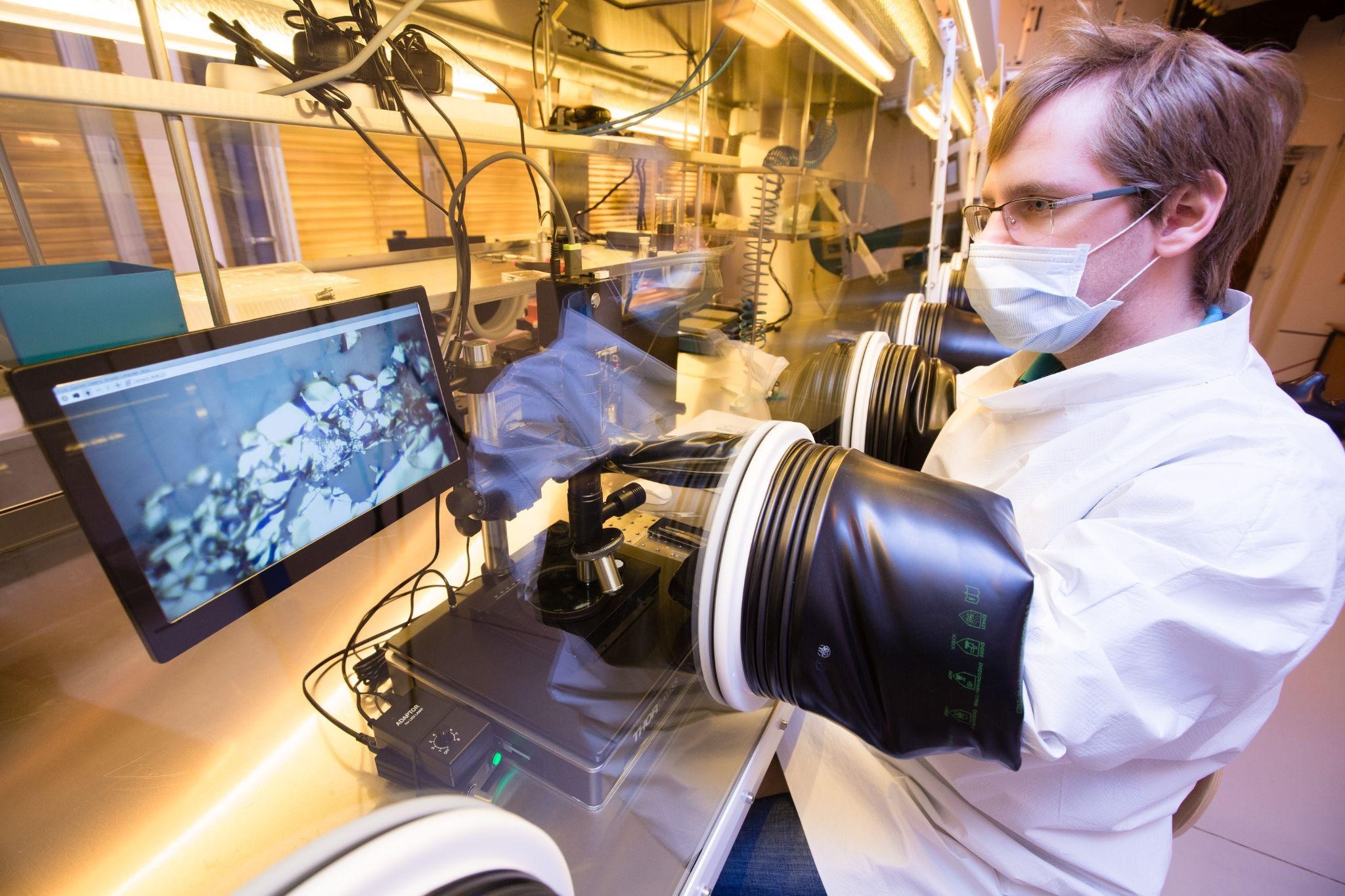
Optical microscopes with precise multi-axis micromanipulators
The optical microscopes are located inside the glove box and are mainly used for the preparation of thin-film devices, assembling heterostructures and routine inspection of the samples at various stages of the manufacturing process when exposure to oxygen or humid atmosphere has to be avoided. A set of long working-distance lenses enables optical control up to 1 μm spatial resolution during precise fine-mechanic work.
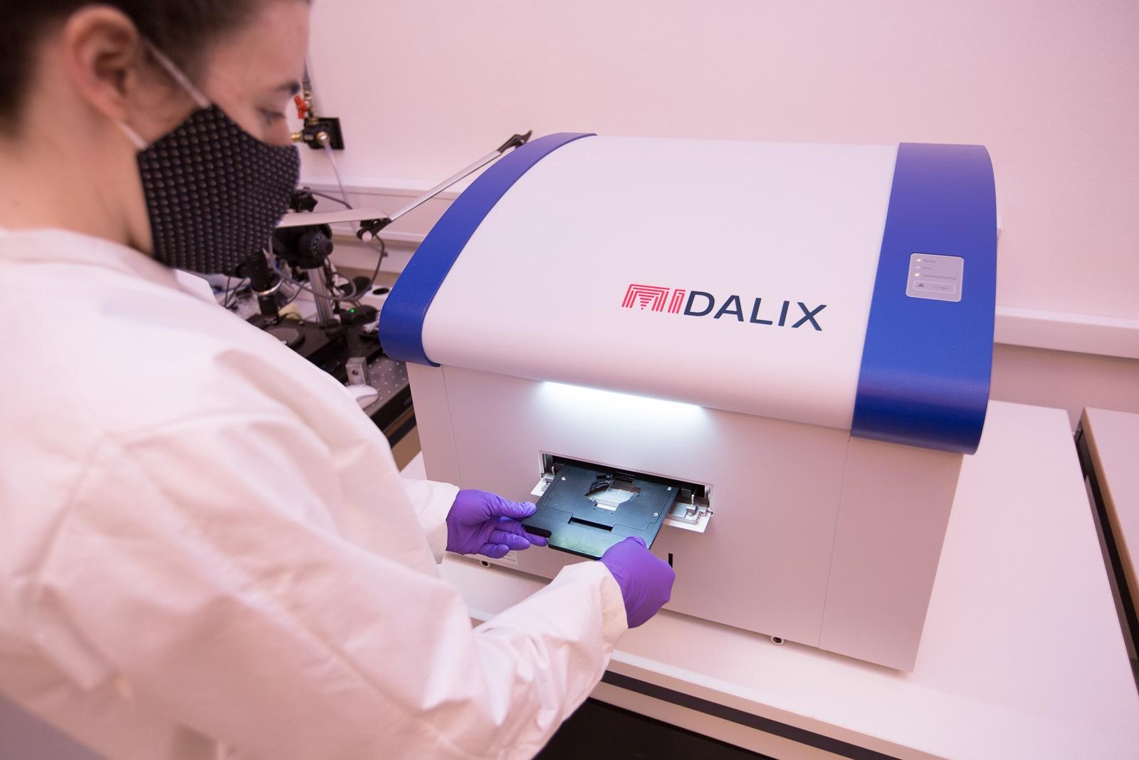
Laser direct imaging system
The miDALIX Dali is a universal, high-resolution, table top laser direct imaging (LDI) system for rapid prototyping on resist-covered substrates. The platform is based on a continuous UV laser, 2D acousto-optical deflectors and a high-precision xy table allowing direct optical lithography with a resolution of 1 µm in a 10×10 cm2 area, which allows fabrication of various types of electronic devices for transport measurements and microfluidic designs. Using 100 kHz beam positioning by acousto-optic deflectors, extremely fast writing is possible. Automated measurements compensate for unevenness of the substrate and applied resists. All job preparation steps are controlled via intuitive software controls. The miDALIX Dali dedicated user interface supports DXF files and also enables CAD design. Different laser tools and algorithms can be selected to optimise the process for speed and the finest structures.
Details:
- Manufacturer: miDALIX
- System: DaLI
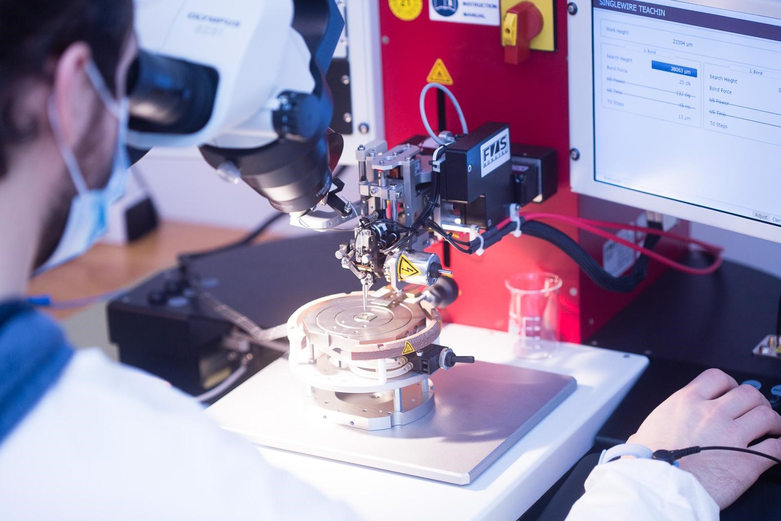
Wire bonder
Semi-automatic wire bonding system with automated Z- and Y-axis produces quick, accurate and reliable electrical connections between the device under test and the sample holder, which is then inserted into a measuring setup. It is primarily used for wedge bonding of aluminium wire with diameter 25 um, but also allows ribbon bonding and ball bonding of golden wire via a built-in heater and flame-off unit. Z-axis maximum distance is 60 mm with 1 μm precision and the biggest length of individual bonds is 20 mm.
Details:
- Manufacturer: F&S Bondtec
- System: 53xxBDA
- Components: 53xx wire bonder, 53xx-BDA bondhead, Olympus stereo-zoom-microscope SZ51
Rapid thermal annealing furnace
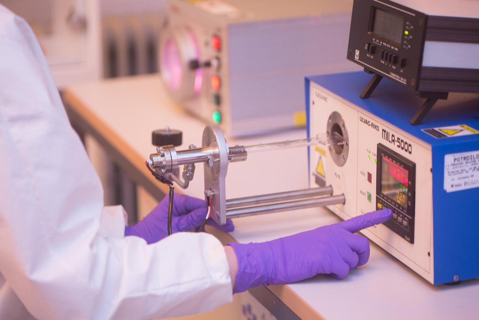
Rapid thermal annealing (RTA) furnace utilises IR radiation to controllably heat up devices in order to improve contact between different materials, promote diffusion of dopants, and activate certain chemical reactions. It allows rapid heating of samples (max. dimensions 20 x 20 mm2) in vacuum or in N2, Ar, O2 and Nitrostar atmospheres up to 1200 ℃.
Details:
- Manufacturer: Ulvac-Riko
- System: Mila-5000
Gas plasma cleaning system
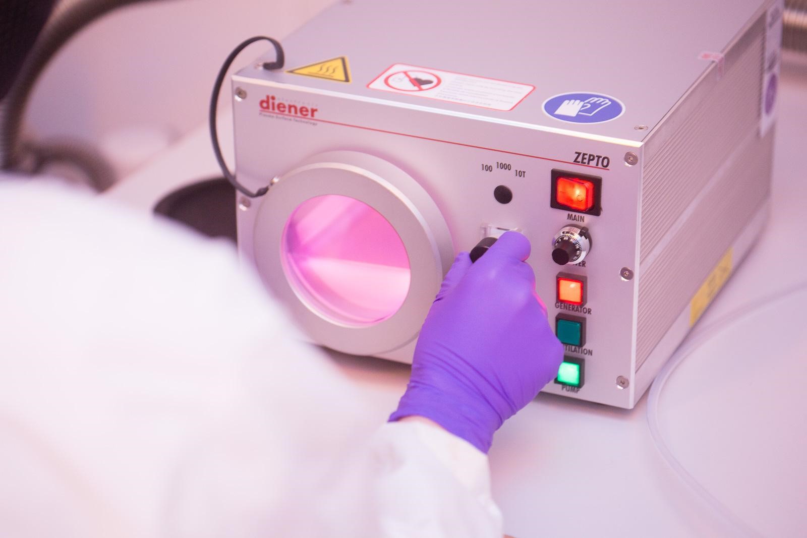
Plasma cleaning is used for removal of surface oxidation and clearing organic residue from surfaces of materials and devices before further processing or measurements. The cleaning process can be performed in air or oxygen plasma, as well as low-pressure air plasma (~1 mbar). The system can also be used to perform plasma activation of surfaces to improve adhesion properties of many materials including metals, ceramics, polymers, etc. Volume of the chamber is ~1.7 L.
Details:
- Manufacturer: Diener electronic
- System: Zepto
Sputtering system
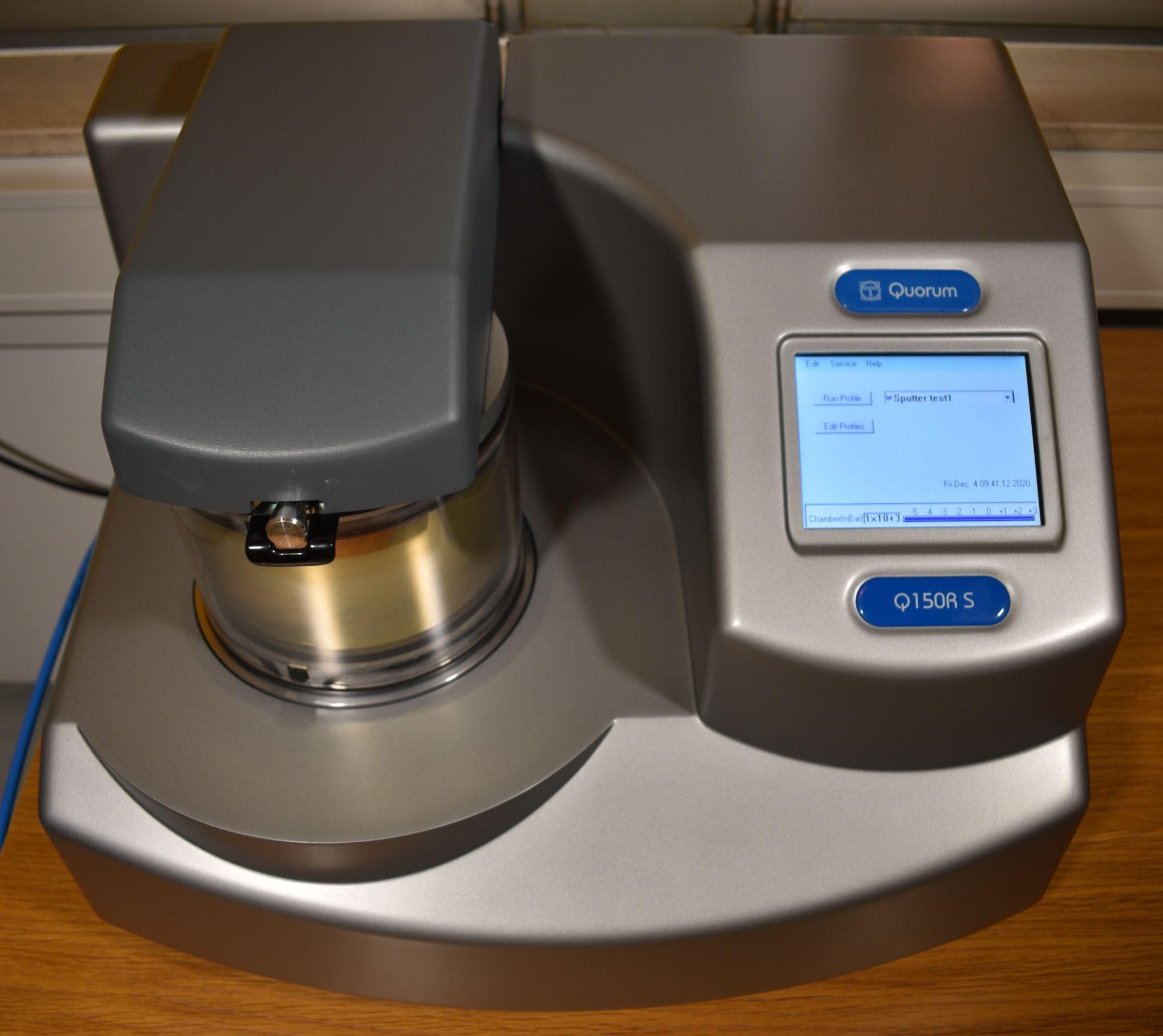
Automated sputter coater for non-oxidising metals used for deposition of thin metal films during the process of device fabrication or for deposition of thin conductive coatings on samples for SEM studies. The system allows sputtering of Au, Au/Pd and Pt metals from disc-style 57 mm diameter targets at vacuum levels between 2×10⁻² and 1×10⁻¹ mbar. Thickness of the deposited film is controlled via a built-in thickness monitor.
Details:
- Manufacturer: Quorum Technologies
- System: Q 150R S
Laminar flow boxes and fume hood
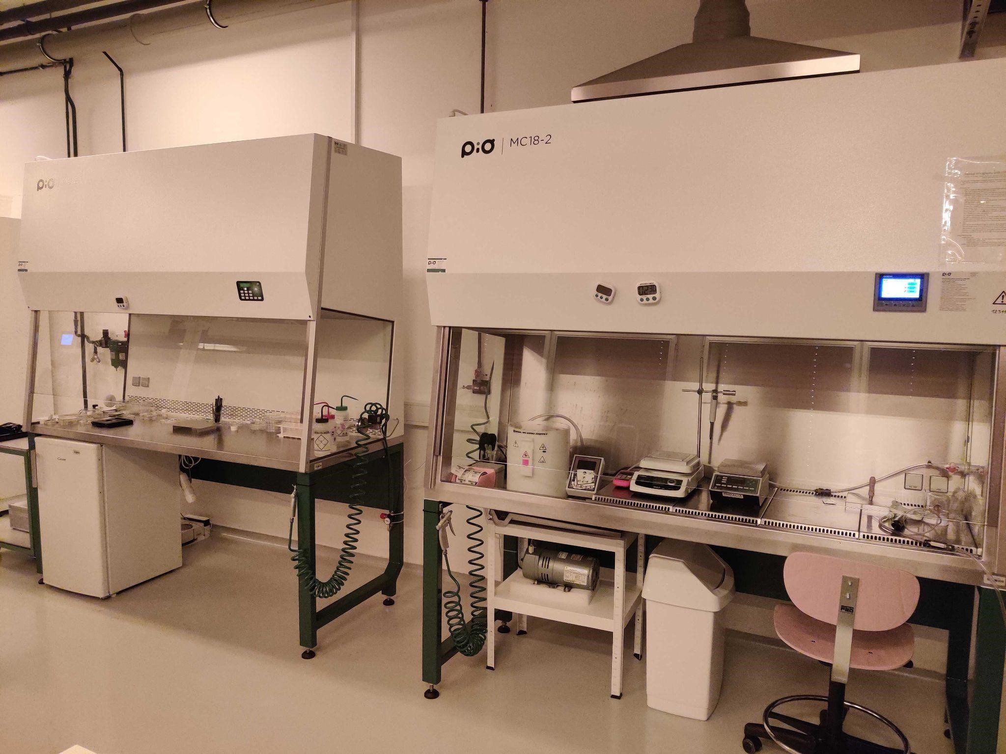
Two flow boxes supply vertical laminar airflow to ensure a clean working surface (ISO 4) for performing lithographic process, such as developing, spin-coating and lift-off. This allows preparation of test sample in a clean atmosphere with reduced concentration of dust particles. One flow box can also operate as a fume hood, which enables safe handling of chemicals.
Details:
- Manufacturer: Iskra PIO
- Systems: MC18-1, MC18-2
- Components: MC18-1 flow box, MC18-2 flow box and fume hood
Cryogenic 4-probe stations (with 2.6 T magnet)
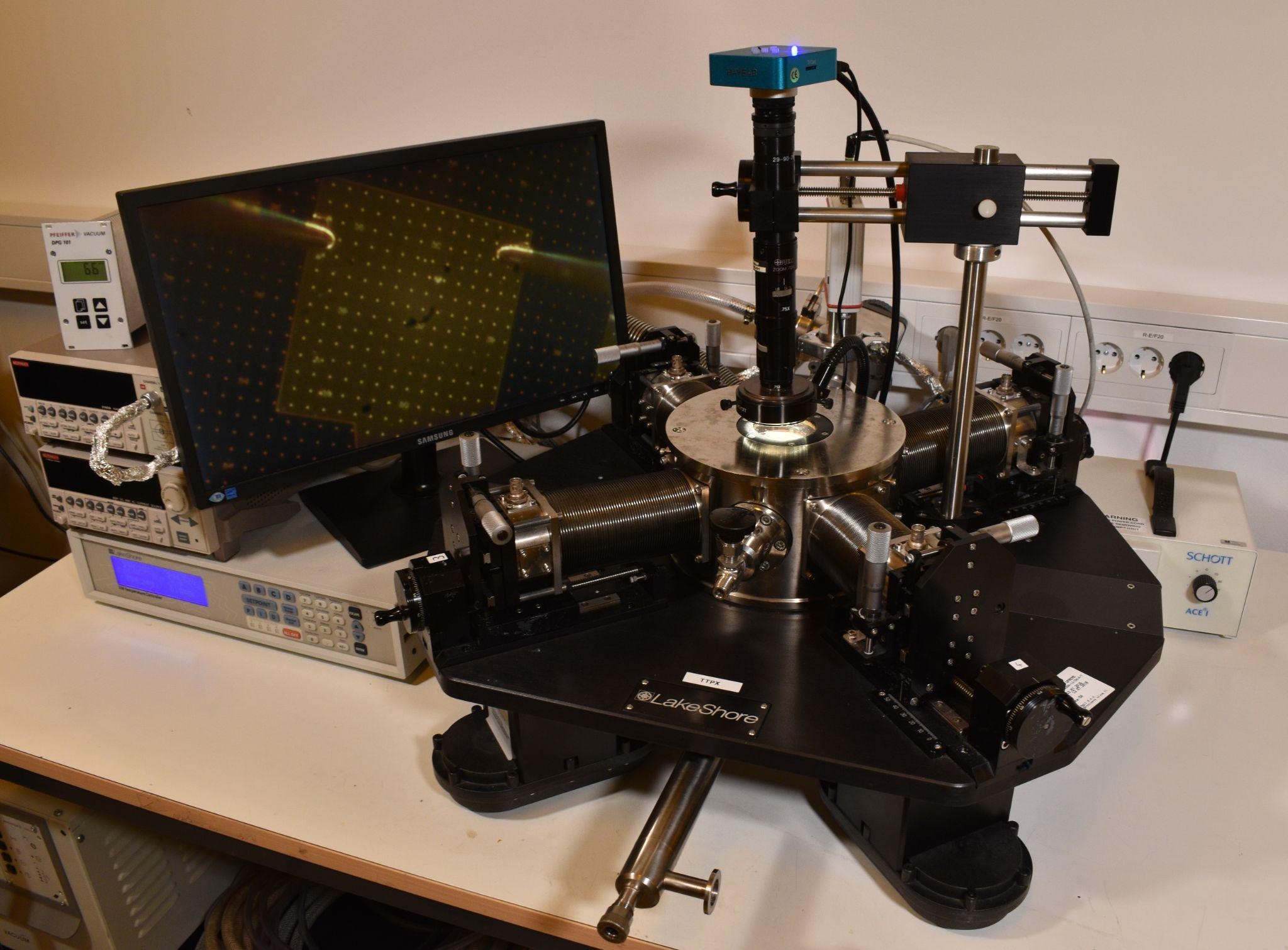
Two cryogenic 4-probe stations for measurements of electrical properties in the temperature range of 4-400 K with optical access; one station also allows vertical magnetic field up to 2.6 T. Each of the four probes can be moved individually in three degrees of freedom with micrometre screws. Each probe is a thin needle-like tip with curvature radius of 25 um, and is connected to the measurement device through a triaxial connector. For cooling, liquid nitrogen or helium can be used, reaching temperatures down to 4 K. Probe stations enable characterisation of many samples during the same cooldown, and can be used for transport measurements of various devices, thin films and even superconducting materials. Electrical measurements can be performed in the frequency range from DC to 1 GHz. For electrical measurements a combination of a current source Keithley 6221 and a nanovoltmeter 2182a is used, which provides accurate resistance measurement, pulsed I-V measurements and differential conductance measurements. Additional electrical pulse excitation of the device under test is possible by using a Siglent arbitrary waveform generator.
Details:
- Manufacturer: Lake Shore Cryotronics
- Systems: TTPX cryogenic probe station, CPX-VF cryogenic probe station with a magnet
- Components: Two cryogenic probe stations (TTPX, CPX-VF), two model 336 temperature controllers, model 625 superconducting magnet power supply, Keithley 6221 current source and Keithley 2182a voltmeter, Siglent SDG1050
Closed cycle cryostations
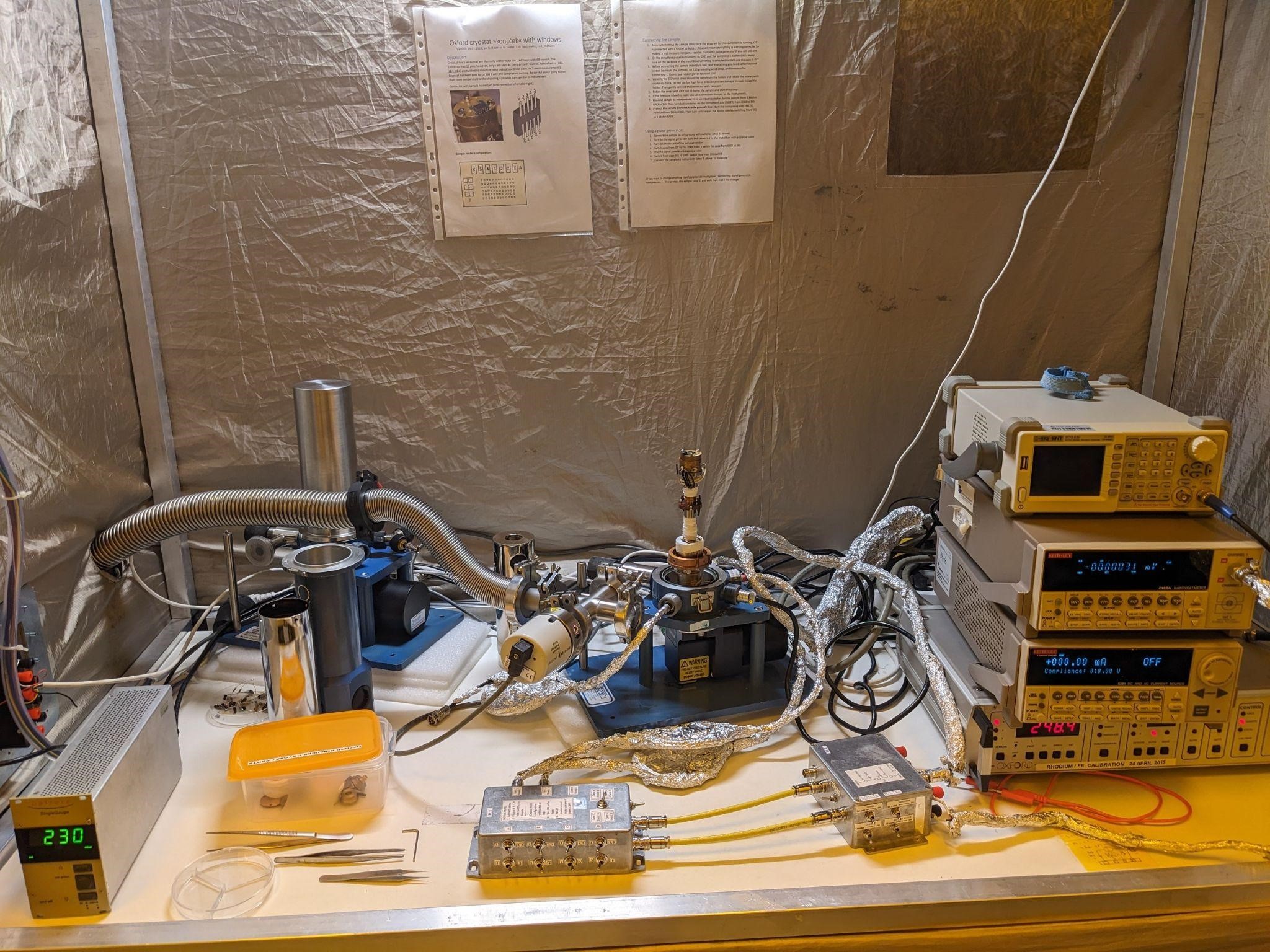
Two helium closed-cycle cryostations for measurements of electrical characteristics in the temperature range of 10-350 K for measurements of transport properties of various devices and thin films. Ease-of-use and closed-cycle cooling capability enable nearly supervision-free operation of the cryostat over extended period of time. Both cryostations are situated in a electromagnetically shielded Faraday tent with filtered cable feedthroughs, which ensure a low-noise experimental environment. For electrical measurements a combination of a current source Keithley 6221 and a nanovoltmeter 2182a is used, which provides accurate resistance measurement, pulsed I-V measurements and differential conductance measurements. Additional electrical pulse excitation of the device under test is possible by using a Siglent arbitrary waveform generator.
Details:
- Manufacturer: Oxford Cryosystems, Oxford Instruments
- Systems: Two Coldhead 2/9 cryostats
- Components: Two Coldhead 2/9, K450 helium compressor, model 503 temperature controller, Keithley 6221 current source and Keithley 2182a voltmeter, Siglent SDG1050
